Alumni Project
Materials for Energy
Workshop
Engineered nanomaterials for next-level technologies
New nanomaterials can be engineered to show unprecedented tunable optical, magnetic, and electronic properties, thereby enabling new functions and improve products in technological applications. These are required, as current technologies are at the limit of the possible miniaturization of their components. To further increase the efficiency of technical devices, alternatives to silicon-based electronics must be sought out. One potential candidate is 2D materials, which refer to materials in which electrons can only move freely on the nanoscale in two dimensions. These materials conduct electricity and heat much better than copper and they are extremely flexible.
Prime examples of the most fascinating functionalities of 2D materials are charge-density waves (CDWs) and high-temperature superconductivity. However, the origin of these attractive (electronic) order phenomena like superconductivity in condensed matter physics is a long-standing debate, and much of it remains unexplained.
Making the leap into application requires further research
Potential new applications of such 2D materials will be in the field of efficient electrical power generation, transmission, and storage; fast and secure communications; medical imaging and treatment; architectures for processing and caching quantum information; and compact solid-state devices, sensors, and actuators.
Exploiting the great potential of nanomaterials and making the leap into application will require further interdisciplinary research. This is because nanomaterials are at the interface of disciplines like biology, chemistry, physics and material sciences. A detailed understanding of the properties of these materials has been hampered due to a combination of factors, such as the lack of clean samples, the challenge to generate and grow high-quality 2D materials, and the absence of high-pressure laboratory work to control the properties of such materials.
Using hydrostatic pressure to change the material’s structure
Pressure in particular is the most successful tuning parameter to change the electronic structure without changing the chemical composition of the material. Applying pressure is the only known way to achieve particular quantum states in 2D materials, which is needed to test and understand their properties. In pressure measurement both the medium and the sample cell must withstand high pressure. Diamonds and materials such as CuBE (copper or beryllium) are often used.
Fast-growing and promising fields in physics that benefits largely from emerging new materials are spintronics and magnonics with great potential related to the improvement of storage capacities and information passage. These technologies rely on nanomaterials with dimensions smaller than the spin/magnon relaxation length.
Focus of the project: Insights into quantum states of new materials
The project provides valuable new insights into the quantum states of new materials while focusing on the synthesized nanomaterials ‛transition metal dichalcogenides’ (TMDs), which are a major class of 2D graphene cognate and high transition-temperature (high-Tc) superconductors.
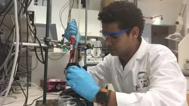
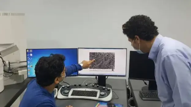
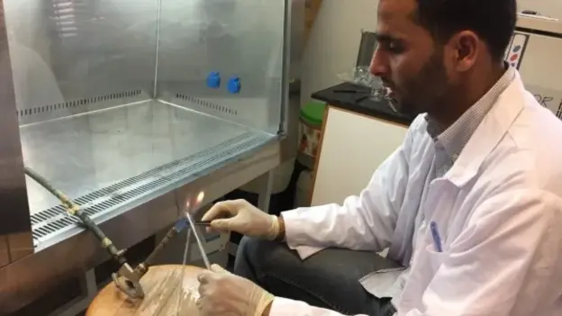
The research on the properties of these materials took place at Goethe University Frankfurt (Germany), the Hashemite University (Jordan), and the University of Fayoum (Egypt) at the newly established low temperature laboratory with a Physical Property Measurements System (PPMS). The laboratory is considered to serve as a platform for future Arab-Arab-German collaborations. Additionally, the theoretical calculations and simulations were carried out at Cairo University in order to contextualize the experimental results. In particular, the results on the superconducting gap values parameter symmetry are further explored by the team of AGYA alumnus Ahmad El-Guindy.
This research project results from previous AGYA projects on emerging materials.
- Disciplines Involved
- Physics, Mathematics
- Cooperation Partners
- Goethe University Frankfurt, Germany
- University of Fayoum, Egypt
- The Hashemite University, Jordan
- Project Title
- Materials for Energy: Research on New Materials for Energy Technology
- Year
- 2020
- Funding Scheme
- Alumni Project
- Countries Involved
- Egypt, Germany, Jordan
- AGYA Publication
- Single-Crystal Growth and Small Anisotropy of the Lower Critical Field in Oxypnictides: NdFeAsO1 - xFx
- Evidence for the Fulde–Ferrell–Larkin–Ovchinnikov state in bulk NbS2
- Sharp Peak of the Critical Current Density in BaFe2−xNixAs2 at Optimal Composition


